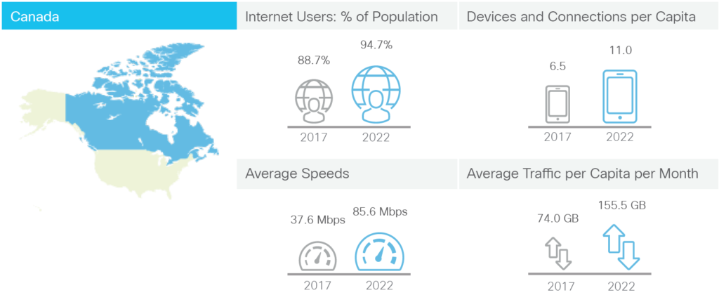
Increasing demand for wireless communication has made spectrum a scarce commodity. Mobile data traffic in Canada is slated to increase 4-fold over 2017 levels by 2022 [1]. In response, the government of Canada is trying to make mmWave bands (26, 28 and 38 GHz) available for high-quality wireless services and innovative 5G applications [2], but this will require commissioning and deploying new equipment at great expense. At the same time, our use of unlicensed spectrum (around 2.4 GHz and 5 – 6 GHz, for example) is growing even faster than that of the licensed spectrum and therefore seeing tremendous congestion. The number of wirelessly connected devices will be more than three times the global population by 2023 [3], and the worldwide energy consumption of communication infrastructure will exceed 3000 TWh/yr with growth at a frightening 7% annually, sharing 20% of the global electricity usage by 2030 [4].
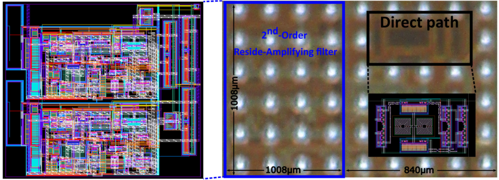
Our research is focused on developing high-speed transceiver circuits to exploit larger bandwidths, make more efficient use of spectrum, and decrease power consumption. Specifically, we are currently focused on the design of the analog-to-digital converters for these applications. For example, a primary challenge in wireless communication is the so-called “near-far” problem whereby many transmitters occupy adjacent channels – some nearby, some far away. Therefore, a tremendous dynamic range is required to receive signals from a faraway source in the presence of much larger interference signals from nearby “blockers” that overwhelm the receiver. In mobile devices, the objective is to isolate the desired channels from adjacent blockers. In the infrastructure (i.e. cell tower), circuitry is required to process all signals, near and far, simultaneously. Both are exciting research opportunities. More specifically, in our research, we present a design methodology for near-Nyquist Continuous-time pipelined (CTP) ADCs [5]. The delay circuit is optimized to match the ADC/DAC path in both its broadband magnitude response and phase. The residue filter response is optimized to prevent image signals from overloading the subsequent stage. We show that practical circuits can extend the band width of the CTP architecture to SRs of 1.5-2.0. The delay and residue-amplifying filter circuits required for a 3 GHz bandwidth ADC are incorporated into a complete 4-bit CTP stage operating at 10 GS/s in a 28nm CMOS prototype. Measurement results confirm that CTP ADC’s performance is at a very competitive oversampling ratio (OSR) of 1.7.
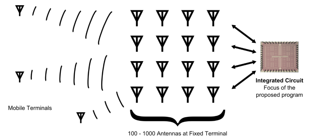
Another objective of our research is to address the fundamental IC implementation problems associated with new wireless communication technologies that rely upon a massive plurality of signal paths through the transmitter and receiver. Specifically, “massive MIMO” (multi-input multi-output) is a wireless technology that relies upon hundreds or even thousands of antennas at the fixed terminals (i.e. central router or base-station) while maintaining only 1-4 antennas in each mobile device. All antennas in the fixed terminal transmit and receive signals in concert to hundreds of users simultaneously using the same frequencies, thereby permitting tremendous reuse of available spectrum. Orders-of-magnitude increases in bandwidth are achievable without increasing spectrum or radiated-power limits. The excellent directivity of massive arrays can also be used to increase the reach of wireless communication, a great benefit for Canada’s remote geographies. The tremendous potential of massive MIMO has made it a key part of wireless technology roadmaps worldwide and implicit in Canada’s wireless regulatory policies, yet that potential is being questioned because the assumed analog signal processing required at the fixed terminals for straightforward implementation of massive MIMO is impractical. Specific challenges include the need for 100’s of precise RF clocks, 100’s of parallel broadband data converters, and their manufacture in low-cost CMOS, which is subject to tremendous variability. The proposed program seeks analog integrated signal processing technologies to address these challenges in future wireless infrastructure, enabling practical and inexpensive massive MIMO communication.
[1] https://www.cisco.com/c/dam/m/en_us/solutions/service-provider/vni-forecast-highlights/pdf/Canada_Consumer_Highlights.pdf
[2] https://www.canada.ca/en/innovation-science-economic-development/news/2022/06/government-of-canada-launches-consultation-on-making-more-spectrum-available-for-high-quality-wireless-services.html
[3] https://www.cisco.com/c/en/us/solutions/collateral/executive-perspectives/annual-internet-report/white-paper-c11-741490.pdf
[4] Andrae ASG, Edler T. On Global Electricity Usage of Communication Technology: Trends to 2030. Challenges. 2015; 6(1):117-157. https://doi.org/10.3390/challe6010117.
[5] M. W. Ismail, H. Shibata, Z. Li, S. Patil and A. Chan Carusone, “A Design Methodology for Achieving Near Nyquist Continuous Time Pipelined ADCs,” IEEE Transactions on Circuits and Systems I: Regular Papers, 2022. [On IEEExplore]