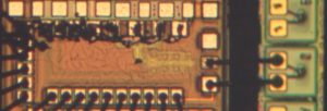
| 112 Gb/s -8.2 dBm Sensitivity 4-PAM Linear TIA with Co-Packaged Photodiodes Designer: Dhruv Patel Technology: 16nm FinFET CMOS This work demonstrates a 112 Gb/s 4-PAM linear TIA in CMOS flip-chip co-packaged with commercial PDs and different PD-to-RX interconnect lengths. D. Patel, A. Sharif-Bakhtiar and A. Chan Carusone, “112 Gb/s -8.2 dBm Sensitivity 4-PAM Linear TIA in 16nm CMOS with Co-Packaged Photodiodes,” Custom Integrated Circuits Conference, Newport Beach, CA, April 2022. | 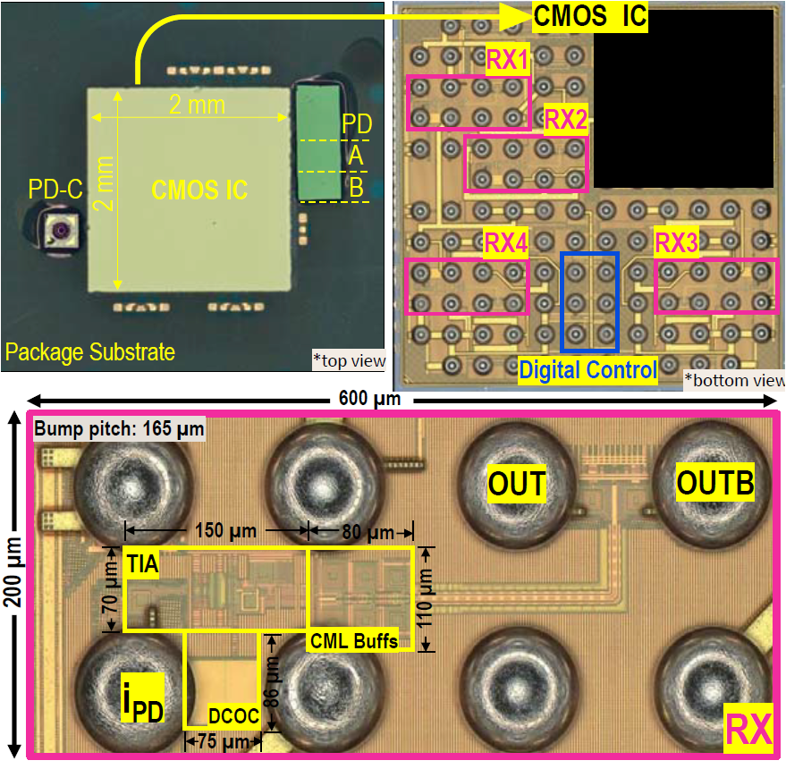 |
| A reconfigurable 5-channel 12-bit RO-based TDC Designer: Foad Arvani Technology: 65nm CMOS A configurable 5-channel RO-based TDC with 31 delay stages in the ring is designed in 65 nm CMOS technology. Sharing the ring oscillator among the five TDC channels reduces the power consumption by more than 75% and area by more than 25% relative to non-shared architecture. F. Arvani and A. Chan Carusone, “A Reconfigurable 5-Channel Ring-Oscillator-Based TDC for Direct Time-of-Flight 3D Imaging,” in IEEE Transactions on Circuits and Systems II: Express Briefs, May 2022. [IEEExplore] |  |
| 2mm-Long 10GHz CMOS Clock Distribution Networks Designer: Xunjun Mo Technology: 16nm FinFET CMOS Two on-die clock distribution networks are used to validate design methodologies for low-jitter CMOS clocking. Circuitry for introducing controlled power-supply noise is included and used to measure the clock distributions’ PSIJ. X. Mo, J. Wu, N. Wary and A. Chan Carusone, “Design Methodologies for Low-Jitter CMOS Clock Distribution,” in IEEE Open Journal of the Solid-State Circuits Society, Oct. 2021. [IEEExplore] |  |
| A 7-GS/s 5-bit Continuous-Time Pipelined Binary-Search Flash ADC Designer: Danial Mohammadi Technology: 28nm CMOS A novel ADC architecture achieves a sampling rate comparable to flash converters, but with reduced input capacitance, power consumption and kickback. The 5-bit prototype has a 2.5-bit first stage, 1.5-bit second stage, and 2-bit final stage allowing for digital correction of interstage errors. Consuming 47mW at 7GS/s in 28nm CMOS, the converter has 15fF differential input capacitance. D. Mohammadi, M. W. Ismai, R. Saha, H. Shibata, Z. Li and A. Chan Carusone, “A 7-GS/s 5-Bit Continuous-Time Pipelined Binary-Search Flash ADC in 28-nm CMOS,” IEEE Solid-State Circuits Letters, 2020. [IEEExplore] |  |
| A 64Gb/s Adaptive ADC-based 4-PAM Receiver Designer: Luke Wang Technology: 16nm FinFET CMOS A 64Gb/s 4-PAM ADC-based receiver front-end with half-rate sampling CTLE and 6-bit ADC (1-bit folding) is designed in 16nm FinFET CMOS. The ADC quantizer is reconfigurable to allow power scaling. L. Wang, Y. Fu, M. LaCroix, E. Chong, A. Chan Carusone, “A 64-Gb/s 4-PAM Transceiver Utilizing an Adaptive Threshold ADC in 16-nm FinFET,” IEEE Journal of Solid-State Circuits, Dec 2018. [PDF] | 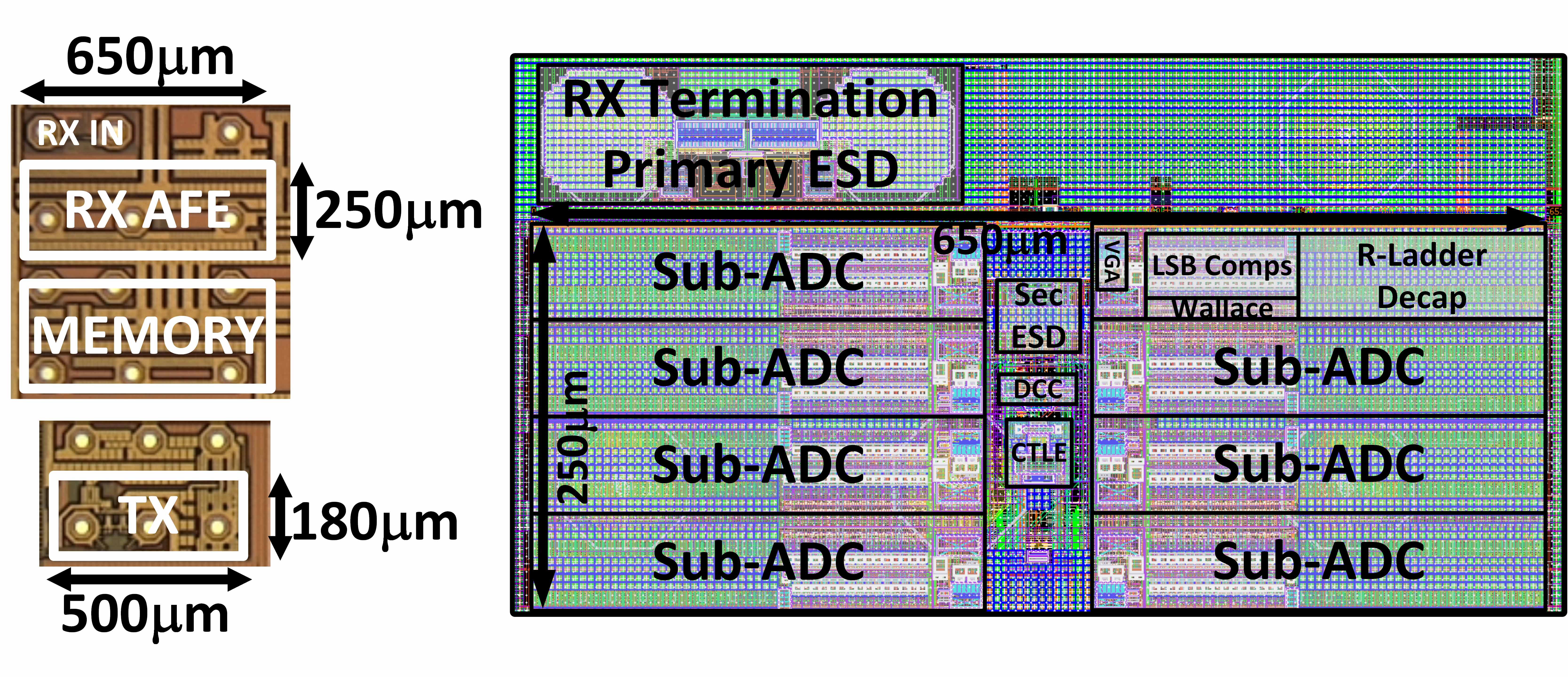 |
| Digital Blocker-Cancelling Receiver for LTE Mobile Handsets Designer: Jeffrey WangTechnology: 28nm CMOS A complete receiver front-end incorporates digital blocker cancellation to extend dynamic range dramatically. Its power consumption scales dramatically with input blocker power.Q. Wang, H. Shibata, A. Liscidini, A. Chan Carusone, “A Digital Filtering ADC With Programmable Blocker Cancellation for Wireless Receivers,” IEEE Journal of Solid-State Circuits, March 2018. [On IEEExplore] | 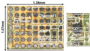 |
| 4GS/s Reconfigurable ADC in 16nm FinFET Designer: Luke Wang Technology: 16nm FinFET CMOS This ADC with VGA is implemented in 16nm FinFET technology and has a resolution programmable from 2 to 6 bits while maintaining state-of-the-art power efficiency. L. Wang, M. LaCroix, A. Chan Carusone, “A 4GS/s Single Channel Reconfigurable Folding Flash ADC for Wireline Applications in 16nm FinFET,” IEEE Transactions on Circuits and Systems II, Dec. 2017. [PDF] | 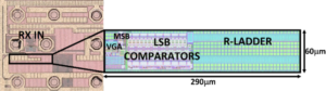 |
| Complete High-Speed CMOS Optical Transceiver Designer: Alireza Sharif-Bakhtiar Technology: 28nm CMOS The transmitter equalizer synthesizes complex-valued poles to compensate for the optoelectronic nonidealities of VCSELs. The receiver employs a high-speed low-noise architecture to achieve a good combination of sensitivity and and power consumption. A. Sharif-Bakhtiar, M. G. Lee, A. Chan Carusone, “A 40-Gbps 0.5-pJ/bit VCSEL Driver in 28nm CMOS with Complex Zero Equalizer,” Custom Integrated Circuits Conference, Austin, Texas, May 2017. [PDF Format]A. Sharif-Bakhtiar, M. G. Lee, A. Chan Carusone, “Low-Power CMOS Receivers for Short Reach Optical Communication,” Custom Integrated Circuits Conference, Austin, Texas, May 2017. [PDF Format] | 
   |
| 16Gb/s Wireline Receiver with Adaptive 1 IIR + 1 Discrete-Time Tap DFE Designers: Shayan Shahramian, Behzad Dehlaghi Technology: 28nm FDSOI CMOS This receiver is the first to demonstrate a practical and fast adaptation method (converging in 5us) for decision feedback equalizers combining IIR and discrete-time taps. S. Shahramian, B. Dehlaghi, A.Chan Carusone, “Edge-Based Adaptation for a 1 IIR + 1 Discrete-Time Tap DFE Converging in 5us,” IEEE Journal of Solid-State Circuits, pp. 3192-3203, Nov 2016. [On IEEExplore] |  |
| 20Gb/s Receiver for Short-Reach Parallel Optical Communication Designer: Alireza Sharif-Bakhtiar Technology: 65nm CMOS An ultra-low-power technique for IIR decision feedback equalization enables 20Gb/s operation consuming only 0.3pJ/bitA. Sharif-Bakhtiar, A.Chan Carusone, “A 20 Gb/s CMOS Optical Receiver with Limited-Bandwidth Front End and Local Feedback IIR-DFE,” IEEE Journal of Solid-State Circuits, pp. 2679-2689, Nov 2016. [On IEEExplore] | 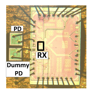 |
| 20Gb/s/wire Parallel Interface Designer: Behzad Dehlaghi Technology: 28nm FDSOI CMOS This receiver establishes a new benchmark for density by combining ultra-compact transceivers consuming only 0.3pJ/bit and a custom-designed silicon interposer.B. Dehlaghi, A.Chan Carusone, “A 0.3 pJ/bit 20 Gb/s/Wire Parallel Interface for Die-to-Die Communication,” IEEE Journal of Solid-State Circuits, pp. 2690-2701, Nov 2016. [On IEEExplore] | 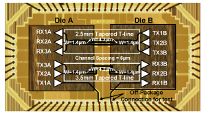 |
| AC-Coupled Laser Diode Driver Designer: Victor Kozlov Technology: 65nm CMOS By demonstrating a laser driver with capacitive AC coupling integrated on-die into a compact area, this design paves the way for the future use of optical I/O in nanoscale CMOS ASICs.V. Kozlov, A.Chan Carusone, “Capacitively-Coupled CMOS VCSEL Driver Circuits,” IEEE Journal of Solid-State Circuits, pp. 2077-2090, Sept 2016. [On IEEExplore] | 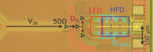 |
| Receiver with Hybrid 2-IIR + 1-Discrete-Time Tap DFE Designer: Shayan Shahramian Technology: 28nm LP CMOS This is the first receiver to combine IIR and discrete-time DFE taps into a single receiver, demonstrating an excellent combination of performance and power considering the LP technology used.S. Shahramian, A.Chan Carusone, “A 0.41 pJ/Bit 10 Gb/s Hybrid 2 IIR and 1 Discrete-Time DFE Tap in 28 nm-LP CMOS,” IEEE Journal of Solid-State Circuits, pp. 1722-1735, July 2015. [PDF Format] |  |
| 26 Gb/s Laser Diode Driver Designer: Masumi Shibata Technology: 65nm CMOS This optical transmitter operates at speeds usually reserved for BiCMOS technologies. It demonstrates that very low power consumption is possible using CMOS circuits and inexpensive packaging.M. Shibata, A. Chan Carusone, “A 26-Gb/s 1.80-pJ/b CMOS-Driven Transmitter for 850-nm Common-Cathode VCSELs,” Optical Fiber Conference (OFC), Los Angeles, California, March 2015. [PDF Format] |  |
| A 2 – 2.5GHz All-Digital PLL Designer: Amer Samarah Technology: 130-nm CMOS A 2–2.5-GHz digital phase-locked loop (DPLL) in 0.13-umCMOS consuming a total of 15.2 mW with a novel stochastic time-to-digital converter. Random jitter as low as 213fs-rms was measured. A. Samarah, A.Chan Carusone, “A Digital Phase-Locked Loop with Calibrated Coarse and Stochastic Fine TDC,” IEEE Journal of Solid-State Circuits, pp. 1829-1841 August 2013. [PDF Format] |  |
| A MASH 1-1-1-1 Delta-Sigma Modulator Designer: Kentaro Yamamoto Technology: 65-nm CMOS The 65-nm CMOS prototype achieves a 70.4 dB peak SNDR over a 2.5-MHz bandwidth while consuming 3.73 mW from a 1.2-V supply. The 276-fJ/conv-step FoM represents a four times improvement over previously-reported delta-sigma modulators using similar zero-crossing-based circuits.K. Yamamoto, A. Chan Carusone, “A 1-1-1-1 MASH Delta-Sigma Modulator with Dynamic Comparator-Based OTAs,”IEEE Journal of Solid-State Circuits, vol. 49, no. 8, pp. 1866-1883, August 2012. [PDF Format] | 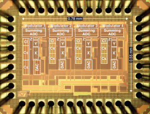 |
| A 2.3-4 GHz Injection-Locked Clock Multiplier Designer: Dustin Dunwell Technology: 65-nm CMOS A frequency-agile multiplying injection-locked oscillator (MILO) suitable for fast power cycling achieves lock over a range of 55.7% around the 3.16-GHz center frequency within 10 reference clock cycles.D. Dunwell, A. Chan Carusone, J. Zerbe, B. Leibowitz, B. Daly, J. Eble, “A 2.3-4 GHz Injection-Locked Clock Multiplier with 55.7% Lock Range and 10-ns Power-On,” Custom Integrated Circuits Conference, San Jose, California, September 2012. [PDF Format] | 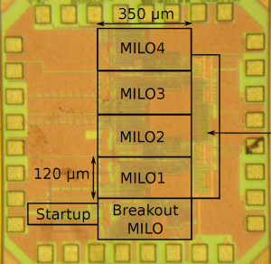 |
| A 7.4 Gb/s 6.8 mW Source Synchronous Receiver Designer: Masum Hossain Technology: 65-nm CMOS This receiver can track very high-frequency jitter on a source-synchronous clock forwarded from a transmitter. Each receiver consumes 0.92 pJ/bit operating at 7.4 Gb/s and has a jitter tolerance of 1.5 UI at 200 MHz.M. Hossain, A. Chan Carusone, “7.4 Gb/s 6.8 mW Source Synchronous Receiver in 65 nm CMOS,” IEEE Journal of Solid-State Circuits, vol.46, no.6, pp.1337-1348, June 2011. [PDF Format] |  |
| A 5-Gb/s Half-Rate Receiver for AC-Coupled Channels Designer: Masum Hossain Technology: 0.18-um CMOS M. Hossain and A. Chan Carusone, “Multi-Gb/s Bit-by-Bit Receiver Architectures for 1-D Partial Response Channels,” IEEE Transactions on Circuits and Systems I: Regular Papers, pp. 270-279, January 2010. [PDF Format] |  |
| Injection-Locked Quadrature Oscillators for GHz Clock AlignmentDesigner: Masum Hossain Technology: 90-nm CMOS This quadrature ring oscillator provides a 2 to 7 GHz clock with controllable phase while consuming 14 mW. M. Hossain and A. Chan Carusone, “CMOS Oscillators for Clock Distribution and Injection-Locked Deskew,”IEEE Journal of Solid-State Circuits, pp. 2138-2153, August 2009. [PDF Format] |  |
| A 32-Gb/s 4-PAM Coaxial Cable Transmitter Designer: Horace Cheng Technology: 0.13-um CMOS This is the fastest 4-PAM transmitter ever demonstrated to date. It incorporates an equalizer capable of compensating for up to 30-dB of cable loss.H. Cheng, F. A. Musa, and A. Chan Carusone, “A 32/16 Gb/s Dual-Mode Pulse Width Modulation Pre-emphasis (PWM-PE) Transmitter with 30-dB Loss Compensation using a High-Speed CML Design Methodology,” IEEE Transactions on Circuits and Systems I: Regular Papers, pp. 1794 – 1806, August 2009. [PDF Format] |  |
| A 35-GS/s, 4-bit Flash ADC Designer: Shahriar Shahramian Technology: 0.18-um SiGe BiCMOS This analog-to-digital converter has has 3.7 ENOB with an effective resolution bandwidth of 8-GHz at a full-scale input of only 270-mVpp differential.S. Shahramian, S. P. Voinigescu, A. Chan Carusone, “A 35-GS/s, 4-bit Flash ADC with Active Data and Clock Distribution Trees,” IEEE Journal of Solid-State Circuits, pp. 1709-1720, June 2009. [PDF Format] |  |
| A 20-Gb/s Coaxial Cable Receiver Designer: Peter Park Technology: 90-nm CMOS This analog front end incorporates a variable gain of up to 31dB and an equalizer with sufficient bandwidth for 20Gb/s data while consuming only 138-mW.P. Park, A. Chan Carusone, “A 20-Gb/s Coaxial Cable Receiver Analog Front-End in 90-nm CMOS Technology,” IEEE Asian Solid-State Circuits Conference, Fukuoka, Japan, November 2008. [PDF Format] | 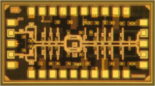 |
| A 40-Gbps 2-Tap Linear Equalizer Designer: George Ng Technology: 0.13-um CMOS This equalizer consumes only 30-mW from a 1.2-V supply and is capable of compensating for channel losses of more than 14-dB at one-half the data rate.G. Ng, A. Chan Carusone, “A 38-Gb/s 2-tap Transversal Equalizer in 0.13-um CMOS using a Microstrip Delay Element,” IEEE RFIC Symposium, Atlanta, George, June 2008. [PDF Format], [PDF Format, slides] | 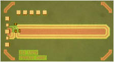 |
| A 3.3-Gbps LDPC Decoder Designer: Ahmad Darabiha Technology: 0.13-um CMOS This is the fastest iterative error control decoder reported to date. It is also capable of decoding with only 150 pJ/bit. A. Darabiha, A. Chan Carusone, and F. Kschischang, “Power Reduction Techniques for LDPC Decoders,” IEEE Journal of Solid-State Circuits, pp. 1835 – 1845, Aug. 2008. [PDF Format] |  |
| Widely Programmable Bandpass DS Modulator Designer: Kentaro Yamamoto Technology: 0.18-um CMOS This design has a centre-frequency programmable from dc to 0.3fs and a peak SNDR of 82 dB.K. Yamamoto, A. Chan Carusone, and F. Dawson, “A Delta-Sigma Modulator with a Widely Programmable Center Frequency and 82-dB Peak SNDR,” IEEE Journal of Solid-State Circuits, pp. 1772 – 1782, Aug. 2008. [PDF Format] |  |
| 14-Gb/s AC-Coupled Receiver Designer: Masum Hossain Technology: 90-nm CMOS This is the highest-speed AC-coupled receiver reported to date with an integrated coupling capacitance below 100-fF.M. Hossain and A. Chan Carusone, “A 14-Gb/s 32 mW AC coupled receiver in 90-nm CMOS,” VLSI Circuits Symposium, Kyoto, Japan, June 2007. [PDF Format] | 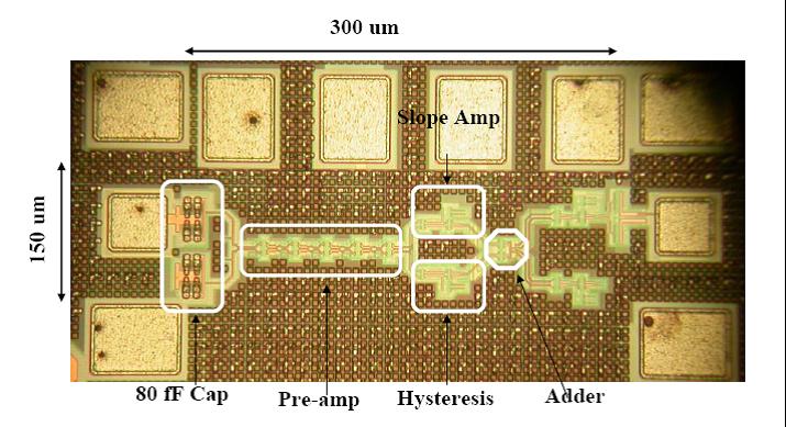 |
| 19-GHz Broadband Amplifier Designer: Masum Hossain Technology: 0.18-um CMOS With a gain of 10-dB, this amplifier has the highest measured bandwidth of any amplifier (with the exception of distributed amplifiers) ever reported in this technology.M. Hossain and A. Chan Carusone, “A 19-GHz Broadband Amplifier Using a gm-Boosted Cascode in 0.18-μm CMOS,” Custom Integrated Circuits Conference, San Jose, California, September 2006. [PDF Format] |  |
| 30-GHz Track-and-Hold Amplifier Designer: Shahriar Shahramian Technology: 0.13-um CMOS With a 30-GHz clock frequency and 7-GHz bandwidth, this is the fastest track-and-hold amplifier ever reported in CMOS. It has a measured THD of -29 dB.S. Shahramian, S. P. Voinigescu and A. Chan Carusone, “A 30-GS/sec Track and Hold Amplifier in 0.13-μm CMOS Technology,” to appear at the Custom Integrated Circuits Conference, San Jose, California, September 2006. [PDF Format] |  |
| 2-GHz CMOS Biquad Filter Designer: Faisal Musa Technology: 0.18-um CMOS This filter has a Q>3 and can be used for equalization and timing recovery at data rates above 3-Gb/s.F. Musa, A. Chan Carusone, “A Baud-Rate Timing Recovery Scheme with a Dual-Function Analog Filter, ” IEEE Transactions on Circuits and Systems II, December 2006, pp. 1393-1397. [PDF Format] |  |
| 40-Gb/s 1-tap Decision Feedback Equalizer Designer: Adesh Garg Technology: SiGe BiCMOS This was, at the time, the fastest DFE ever reported, tested up to 40-Gb/s. It occupies an area of 1.5mmX1mm and operates from a 3.3V supply with 230mA current.A. Garg, A. Chan Carusone, S. Voinigescu, “A 1-Tap 40-Gbps Look-ahead Decision Feedback Equalizer in 0.18μm SiGe BiCMOS Technology,” IEEE Journal of Solid-State Circuits, October 2006, pp.2224-2232. [PDF Format] | 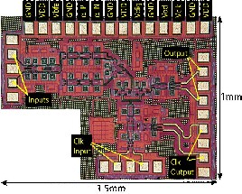 |
| 40-Gb/s 3-tap Linear Equalizer Designer: Jonathan Sewter Technology: 0.18-um CMOS This was the fastest linear equalizer ever reported in any CMOS process at the time. It consumes 70 mW from a 1.8 V supply in an area 1 mm x 1 mm.J. Sewter and A. Chan Carusone, “A 3-Tap FIR Filter with Cascaded Distributed Tap Amplifiers for Equalization up to 40 Gb/s in 0.18-mm CMOS,” IEEE Journal of Solid-State Circuits, August 2006, pp. 1919-1929. [PDF Format] |  |
| 30-Gb/s 3-tap Digitally Programmable Linear Equalizer Designer: Jonathan Sewter Technology: 90-nm CMOS At the time of its publication, this was the fastest linear equalizer reported in any CMOS technology. Consuming only 25 mW from a 1-V supply, and fitting into an area 0.3 mm2, the equalizer has a a serial digital interface to set the tap gains. J. Sewter and A. Chan Carusone, “A CMOS Finite Impulse Response Filter with a Crossover Traveling Wave Topology for Equalization up to 30 Gb/s,” IEEE Journal of Solid-State Circuits, April 2006, pp. 909-917. [PDF Format] |  |