In modern wireline transceivers, many critical architectural aspects should be considered to overcome tomorrow’s 200 Gbps transceiver challenges including physical channel impairments and algorithms required for robust links. At ISL, we focus on chip input and output (I/O) challenges to meet increasing demands for information processing. In addition, we work on integrating reconfigurable and efficient digital signal processing (DSP) to support high speed communication links. Furthermore, our research strives to address the challenges of converting high-speed electrical signals to/from optical signals to achieve optical interfaces at serial data rates of 100+ Gbps.
Die-to-die interconnect:
This research thrust looks at the major challenge facing computer and networking systems now and for the next decade: interconnect energy efficiency. Aggregate interconnect input-output (I/O) bandwidth must increase aggressively to take full advantage of tomorrow’s highly parallel processors, but the total power available for I/O is constrained. In particular, network data traffic patterns pose a difficult problem: how do we maintain energy efficiency in the presence of widely varying bandwidth demands? No single strategy appears to offer the energy-efficiency improvements that will be required in the next decade. Rather, the entire system must be co-optimized including the channel, transmitter, receiver, and clocking circuits, with the objective function being energy consumption per communicated bit. This optimized system must then exploit a combination of power management techniques including burst-mode operation, low-power standby, dynamic voltage and frequency scaling, and dynamic link narrowing.
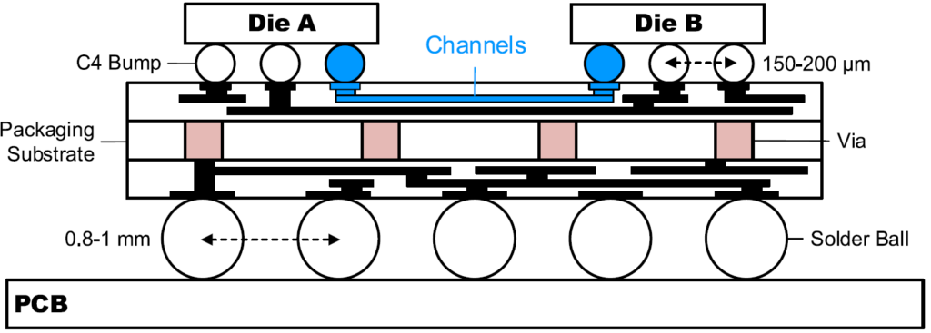
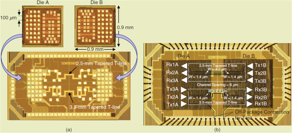
Our research looks at several possible solutions. For example, there are significant potential benefits for co-packaging dies to shorten the length of the links between them, as shown in figure 1. We have already demonstrated state-of-the-art energy efficiency and density over such ultra-short-reach (USR) die-to-die links [1,2]. The transceiver prototype includes 3 transmitters and 3 receivers fabricated in 28 nm STM FD-SOI CMOS technology (figure 2). The parallel interface operates at 20 Gb/s/wire and 18 Gb/s/wire data rates over the 2.5 mm and 3.5 mm channels with 5.9 and 7.7 dB of loss relative to DC at fbit/2 while consuming 0.30 and 0.32 pJ/bit excluding clocking circuits, respectively.
In addition, with CMOS buffers being increasingly used for the distribution of precise clocks in advanced technologies, it is important to understand their limitations and explore design tradeoffs. Our research provides quantitative analyses of the main sources of jitter in CMOS clock distribution: power supply induced jitter, jitter generation, and jitter amplification [3]. Minimizing the number of buffers along the clock distribution network while still maintaining fast rise-fall times and ensuring proper settling of all clock waveforms will minimize the impact of all jitter sources. Following these guidelines can simultaneously reduce power supply noise sensitivity and power consumption of the clock distribution circuits. These conclusions are backed up by simulation and measurement results of two prototype 2-mm long CMOS clock distribution networks designed in 16-nm FinFET.
[1] B. Dehlaghi, A.Chan Carusone, “A 0.3 pJ/bit 20 Gb/s/Wire Parallel Interface for Die-to-Die Communication,” IEEE Journal of Solid-State Circuits, pp. 2690-2701, Nov 2016. [On IEEExplore]
[2] B. Dehlaghi, N. Wary, A. Chan Carusone, “Ultra-Short-Reach Interconnects for Die-to-Die Links: Global Bandwidth Demands in Microcosm,”IEEE Solid-State Circuits Magazine, pp. 42-53, 2nd Quarter, 2019. [On IEEExplore]
[3] X. Mo, J. Wu, N. Wary and A. Chan Carusone, “Design Methodologies for Low-Jitter CMOS Clock Distribution,” Invited to IEEE Open Journal of the Solid-State Circuits Society, Oct. 2021. [Open Access on IEEExplore]
DSP‐Based Transceiver Architectures:
Our research aims to enable the continued proliferation of broadband communication technology by integrating robust, reconfigurable, and efficient digital signal processing (DSP) into our highest speed communication links over copper wires and optical fiber. Multi-Gbps transceivers generally rely upon analog signal processing to condition the communication waveforms, compensating for channel impairments and eliminating noise introduced along the way. Although DSP can offer the improvements in signal integrity needed for long channels and higher data rates, the associated power consumption can be excessive, especially when the channel happens to be short. It is impractical to tailor different transceiver circuits for each of the hundreds of different channels that may arise in a network. Hence, our vision is of reconfigurable transceiver circuits for wireline communication that leverage a flexible DSP and perform efficient communication at 100+ Gbps over a wide variety of channels [1,2].
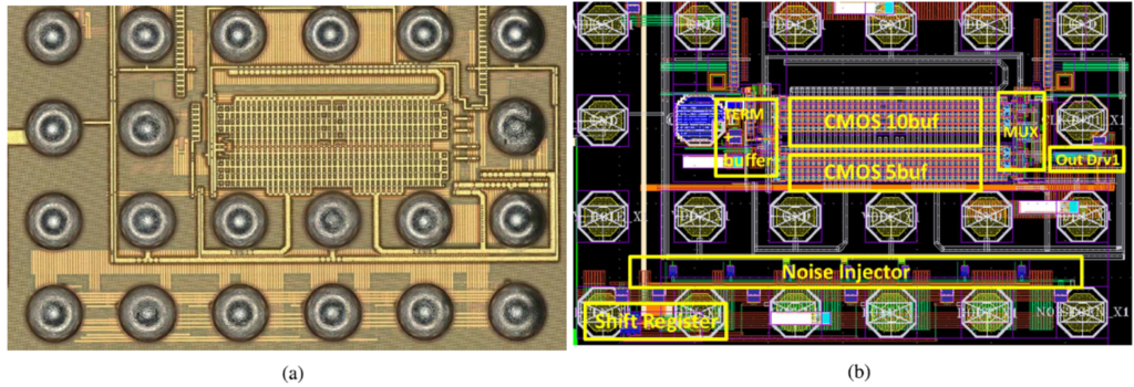
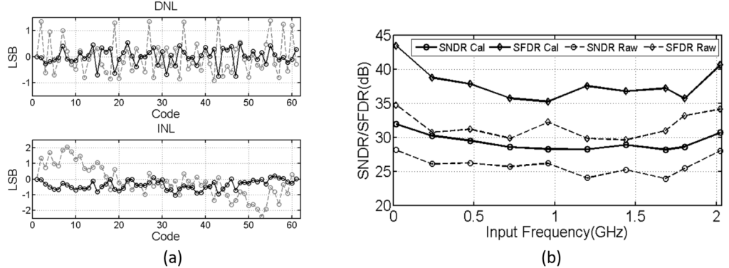
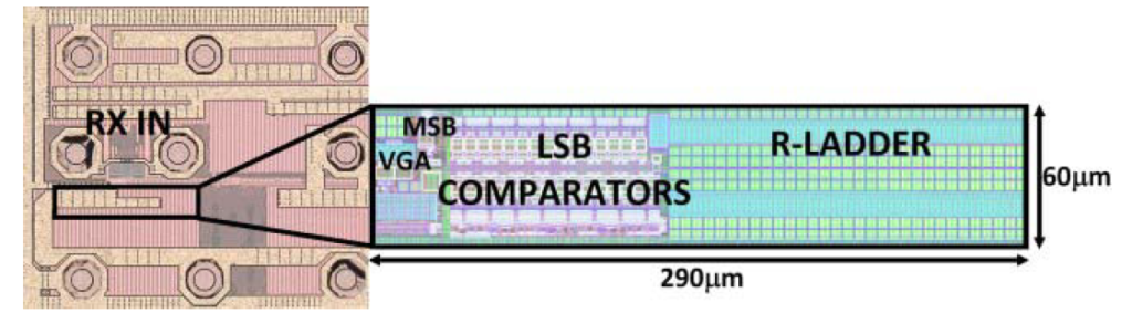
We have already demonstrated the analog front-end circuits, including high-speed data converters, needed for such links. Since the analog circuits are being followed by a sophisticated DSP, digital calibration is a valuable tool in such systems, and a key part of our research. The improvement offered by calibration is illustrated in figure 4. The ADC is fabricated in the TSMC 16nm FinFET CMOS process and the die photo and layout floorplan are shown in figure 5 with a total active area of approximately 60μmx290μm [3]. In another work, we show the results from an ADC reconfigurable from 2- to 6-bits of resolution. Further improvements have been demonstrated in [4]. Our work in this area employs nanoscale CMOS (including FinFET) VLSI fabrication technologies to make state-of-the-art contributions.
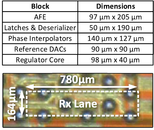
Moreover, we improve the power efficiency of 56Gb/s PAM-4 Wireline Receiver by designing an AFE associated with extensive programmability combined with an efficient genetic adaptation algorithm to select a setting that minimizes BER thus equalizing a 22dB-loss channel [5]. The lack of a DFE, combined with a novel PAM- 4 clock recovery scheme greatly reduces the number of latches required compared to previous works, resulting in 1.41pJ/bit power consumption in 7nm CMOS technology. A chip photo with area breakdown is shown in Figure 6.
In addition, we present an accurate and efficient methodology for optimizing high-speed wireline links and the substantial improvement obtained by using post-FEC vs. pre-FEC BER for optimization [6]. A statistical model that accounts for FFE noise enhancement, DFE burst errors and other important noise sources finds the pre-FEC and post-FEC BER that serve as objective functions for optimizing each transceiver equalizer block. The statistical model can accurately estimate post-FEC BER using standard linear block codes. A genetic algorithm is combined with the statistical model to obtain the best set of design parameters for each transceiver block.
[1] L. Wang, Y. Fu, M. LaCroix, E. Chong, A. Chan Carusone, “A 64-Gb/s 4-PAM Transceiver Utilizing an Adaptive Threshold ADC in 16-nm FinFET,” IEEE Journal of Solid-State Circuits, Dec 2018. [PDF]
[2] L. Wang , Y. Fu , M. LaCroix , E. Chong , A. Chan Carusone, “A 64Gb/s PAM-4 Transceiver Utilizing an Adaptive Threshold ADC in 16nm FinFET,” International Solid-State Circuits Conference, Feb. 2018.
[3] L. Wang, M. LaCroix, A. Chan Carusone, “A 4GS/s Single Channel Reconfigurable Folding Flash ADC for Wireline Applications in 16nm FinFET,” IEEE Transactions on Circuits and Systems II, Dec. 2017. [On IEEExplore]
[4] P. Chen, N. Wary, L. Wang, Q. Wang, A. Chan Carusone, “All-Digital Calibration Algorithms to Correct for Static Non-Linearities in ADCs,” IEEE International Symposium on Circuits and Systems, Seville, Spain, October 2020. [PDF] [YouTube]
[5] S. Shahramian*, B. Dehlaghi*, J. Liang, R. Bespalko, D. Dunwell, J. Bailey, B. Wang, A. Sharif-Bakhtiar, M. Ferrell, K. Tang, A. Chan Carusone, D. Cassan, D. Tonietto, “A 1.41pJ/b 56Gb/s PAM-4 Wireline Receiver Employing Enhanced Pattern Utilization CDR and Genetic Adaptation Algorithms in 7nm CMOS,” International Solid-State Circuits Conference, February 2019. (* Equally credited authors) [PDF]
[6] M. Yang, S. Shahramian, H. Wong, P. Krotnev, A. Chan Carusone, “Global Optimization of Wireline Transceivers for Minimum Post-FEC vs. Pre-FEC BER,” DesignCon, August 2021. (Best Paper Award) [PDF Paper] [PDF Slides]
Optical transceivers:
Traditional electrical interconnects suffer frequency-dependent attenuation. Inside networking and computing infrastructure (large data centers), these losses limit the length of electrical interconnect to as little as a few meters at modern data rates. Moreover, at high frequencies electrical interconnect and connectors act as both transmit and receive antennae, and therefore experience significant crosstalk. Crosstalk limits the density with which high-speed electrical interconnect can be packed. By contrast, signals propagating on optical fibers exhibit relatively little frequency-dependent loss and practically no crosstalk. Counteracting these benefits are the challenges of converting high-speed electrical signals to/from optical signals. Our research strives to address these challenges by developing low-power compact CMOS circuits for optical interfaces at serial data rates of 100+ Gb/s.
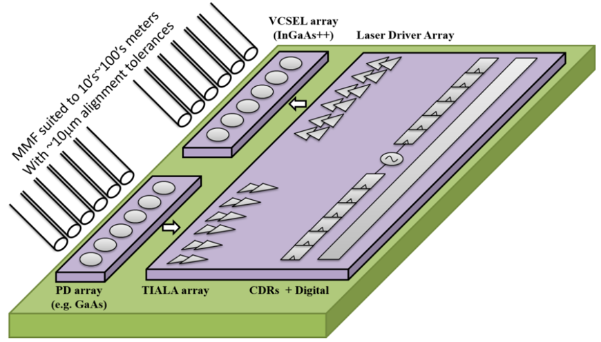
Although the fiber itself may offer a near-ideal medium for optical signal transmission, the optoelectronic devices at either end of the fiber (photodetector, laser, modulator, etc.) can be significant impairments. Firstly, the devices’ electro-optical conversion is inherently inefficient, so the electrical signal induced at the receiver is a small fraction of the electrical signal in the transmitter. Optoelectronic devices also introduce frequency-dependent loss, although unlike the frequency-dependent losses of copper interconnect, this characteristic doesn’t depend upon the length of the interconnect. Finally, nonlinearity of the optoelectronic devices can come into play. Our research strives to overcome these unique challenges using low-cost and low-power CMOS circuits, thus allowing high-performance computing and networking infrastructure to benefit from optical interconnects.
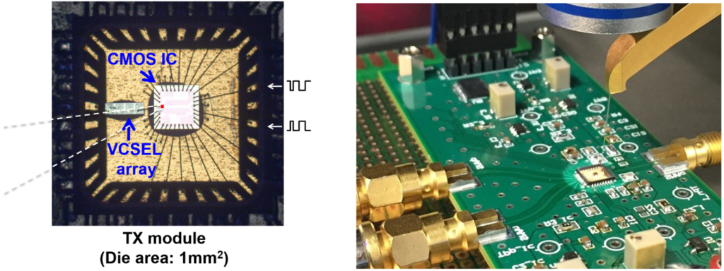
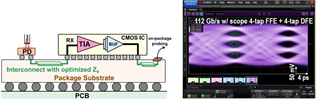
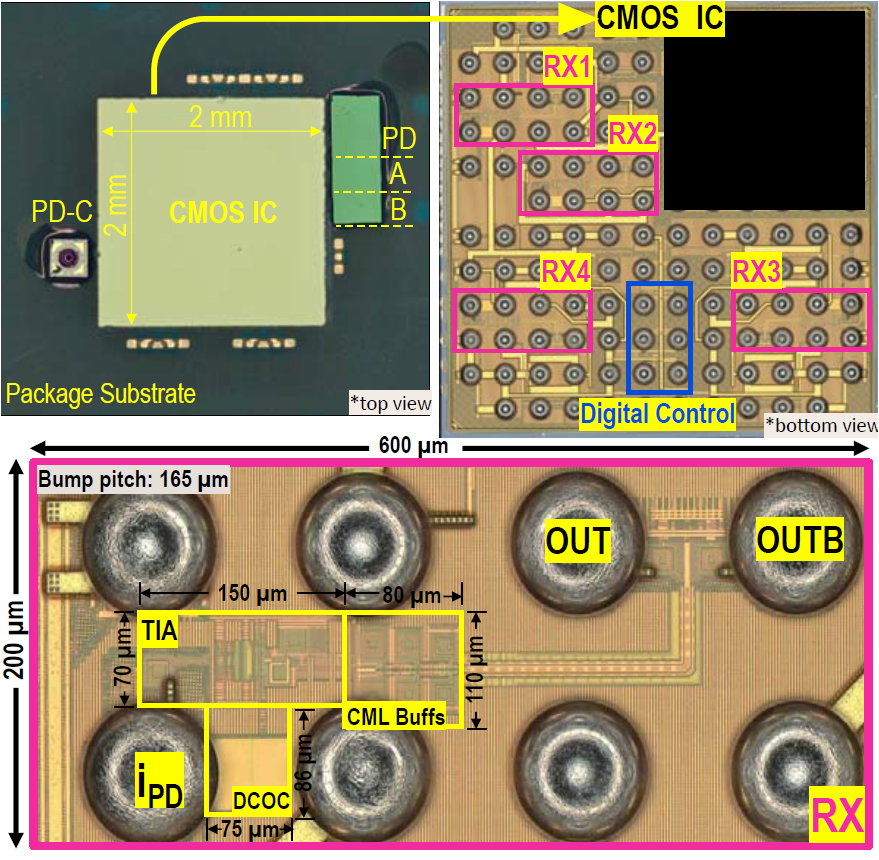
Our recent past work we demonstrated a 26-Gb/s, 1.80-pJ/b transmitter composed of a 65-nm bulk-CMOS driver and an 850-nm VCSEL array in a QFN package. The VCSEL’s anode is directly modulated without a negative supply voltage at 0.82-dBm OMA. Figure 8 shows the photo of the transmitter (left) and the photo of the optical test setups (right). Furthermore, we recently demonstrated a 112 Gb/s 4-PAM linear TIA in CMOS flip-chip co-packaged with commercial PDs and different PD-to-RX interconnect lengths as shown in figure 9 [2]. The eye diagram of one receiver after on-scope 4-tap FFE + 4-tap DFE equalization is shown in figure 9 (right). As shown in the die micrograph (figure 10), two commercial back illuminated InP PD ICs are flip-attached onto the package substrate alongside the CMOS prototype TIAs. The RX prototype is fabricated in 16nm CMOS FinFET.
In addition, we studied the optimization of the frontend of optical receivers [3]. We investigated different optimization techniques used and quantified the optimal bandwidths for 2-PAM and 4-PAM signaling. We found that the optimal bandwidth relative to the baud rate is higher in the case of 4-PAM modulation, but it is lower relative to the bit rate. We covered continuous-time linear equalization (CTLE), feed-forward equalization (FFE), and decision feedback equalizer (DFE)-based optical receivers. we compared these equalization techniques and we reviewed recent advances in optical receiver design with emphasis on 4-PAM optical receivers.
[1] M. Shibata, A. Chan Carusone, “A 26-Gb/s 1.80-pJ/b CMOS-Driven Transmitter for 850-nm Common-Cathode VCSELs,” Optical Fiber Conference (OFC), Los Angeles, California, March 2015. [PDF]
[2] D. Patel, A. Sharif-Bakhtiar, A. Chan Carusone, “A 112Gbps -8.2dBm Sensitivity 4-PAM Linear TIA in 16nm CMOS with Co-Packaged Photodiodes,” Custom Integrated Circuits Conference, Newport Beach, California, April 2022. (Best Student Paper Award) [YouTube]
[3] B. Radi, D. Abdelrahman, O. Liboiron-Ladouceur, G. Cowan and A. Chan Carusone, “Optimal Optical Receivers in Nanoscale CMOS: A Tutorial,” IEEE Transactions on Circuits and Systems II: Express Briefs, April 2022. [Open Access on IEEExplore]