Due to the complexity of digital and analog circuit design in advanced applications such as in high-speed wireline links (beyond 100 Gb/s), a huge number of parameters must be carefully set during the design phase to achieve the desired performance. In addition, dynamic optimization of these parameters is also required during operation to maintain the performance under variable circumstances. Therefore, advanced automated optimization techniques are needed to explore impossibly complex design spaces to find solutions with optimal price, performance, and power (PPP) and unleash engineers’ creativity by quickly identifying alternative solutions that allow for subtle PPP tradeoffs.
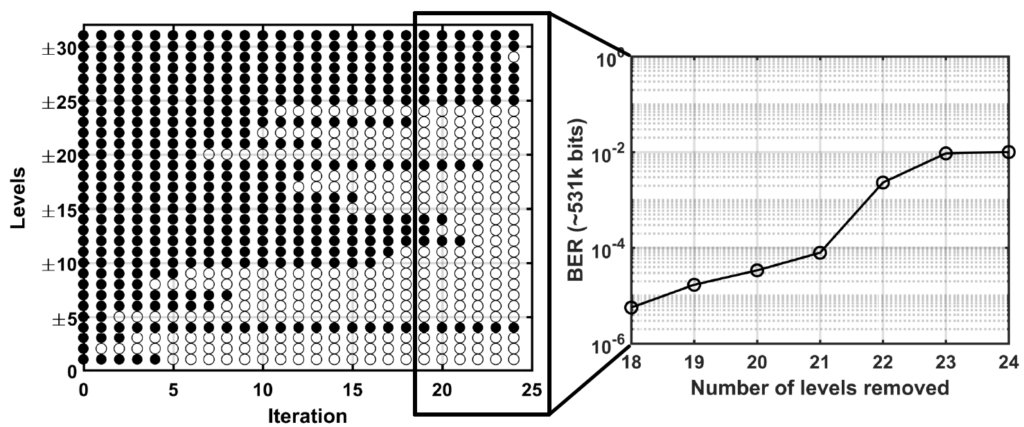
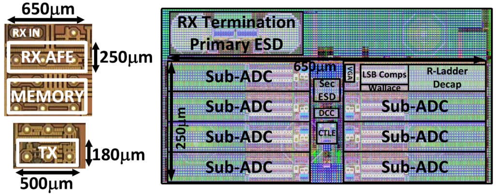
A greedy search technique is an optimization approach that has been demonstrated to reduce the power consumption and improve the bit error rate of high data rate transceivers. In our research, the greedy search approach allows us to shorten the search time and select non-uniform thresholds of analog-to-digital converter (ADC) in the receiver side of a 64-Gb/s 4-pulse-amplitude modulation (PAM) transceiver to reduce the power at low channel loss and to achieve better BER than a uniform quantizer [1]. As shown in Figure 1, the iterative search works by selecting a subset of the candidate levels at each step and using that subset as candidates for the subsequent iteration. The search begins with all threshold levels active and the link operating at a BER well below the target. After iteration 18, the BER increases dramatically above 10−5, and the search can be terminated. The prototype transceiver was fabricated in a TSMC 16-nm FinFET CMOS process. The die photograph and the RX-AFE layout floor plan are shown in Figure 2.
The genetic algorithm (GA), which is an evolutionary algorithm inspired by the law of natural selection, is an efficient technique that can be used as a global optimizer. We have presented an accurate and efficient methodology for using the GA to optimize high-speed wireline links. A genetic algorithm is combined with the statistical model to obtain the best set of design parameters for each transceiver block [2]. Because the GA optimizer explores the entire solution space, it is likely to explore more local minima. Figure 3 presents the pre-FEC BER performance surface showing multiple local minima. The results show that GA can successfully find equalizer coefficients that lead to the globally optimal BER.
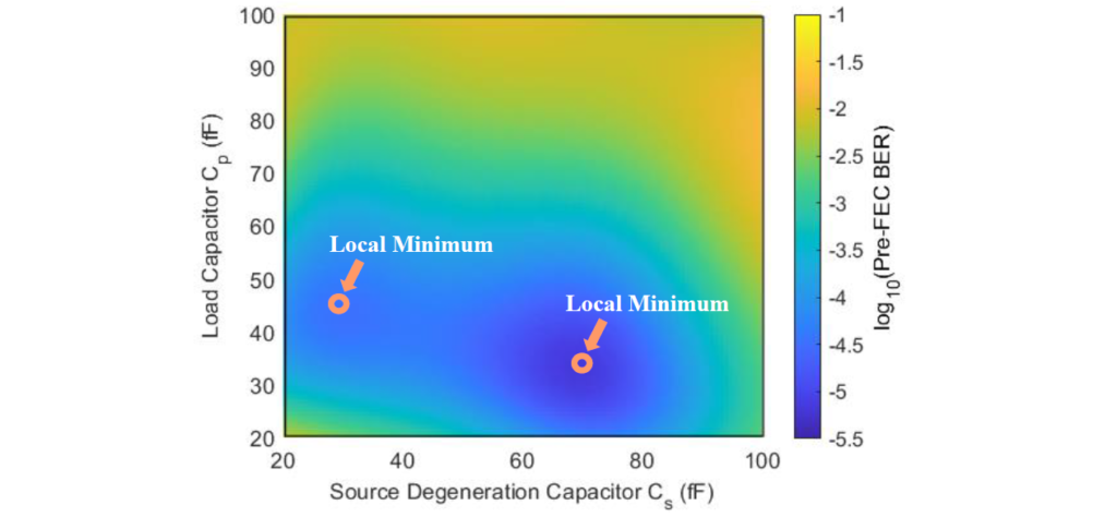
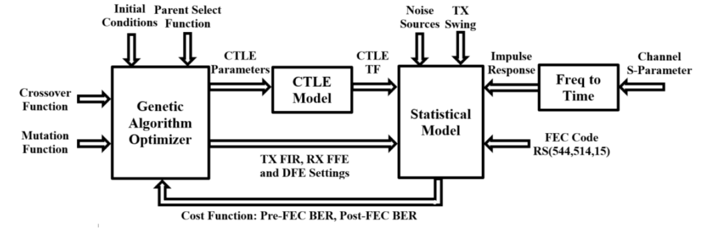
Figure 4 depicts the proposed methodology for wireline transceiver optimization. The optimization framework shown in the diagram includes a statistical model and a genetic-algorithm optimizer, respectively. The GA optimizer can accept customized initial conditions, a crossover/mutation function and a parent-select function. The calculated BERs are used as the cost function to select parents of each new generation. The entire flow can be easily parallelized in software, allowing us to generate and evaluate multiple children simultaneously.
In parallel, we propose in our research for the first time a digital mismatch calibration for quantized analog (QA) signal processing using a genetic algorithm [3]. We propose the genetic algorithm to find non-uniform slicer levels offering superior performance compared to uniform levels. The proposed optimization algorithm can achieve 3 dB higher SNDR by taking advantage of non-uniform quantization under a multitone input.
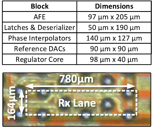
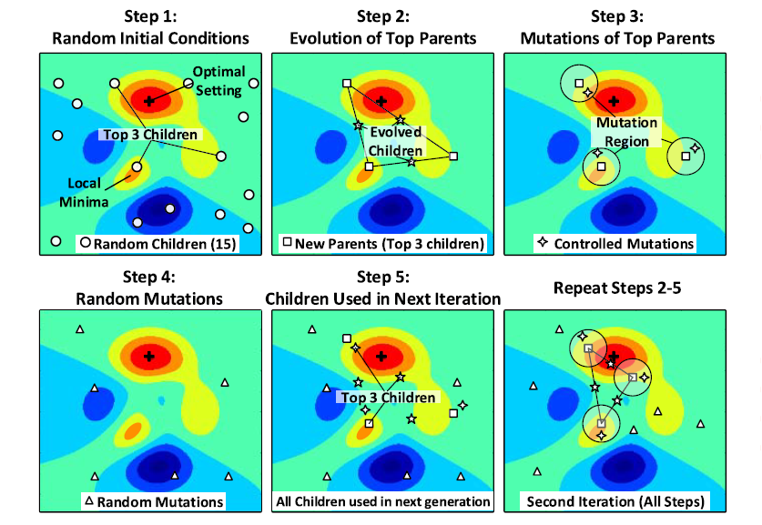
In addition, we used the genetic adaptation algorithm to find the global minima for the bit-error-rate (BER) and optimize the settings of analog front-end (AFE) implemented in 56-Gb/s analog-mixed signal pulse amplitude modulation (PAM)-4 receiver [4]. The optimized AFE results in a low energy consumption of 1.41 pJ/bit. The receiver was fabricated in TSMC 7-nm FinFET CMOS technology. The die photograph of the chip, along with the area breakdown, is shown in Figure 5. Figure 6 illustrates the genetic adaptation algorithm procedure for optimization of the AFE parameters on a 2-D performance surface to allow better visualization.
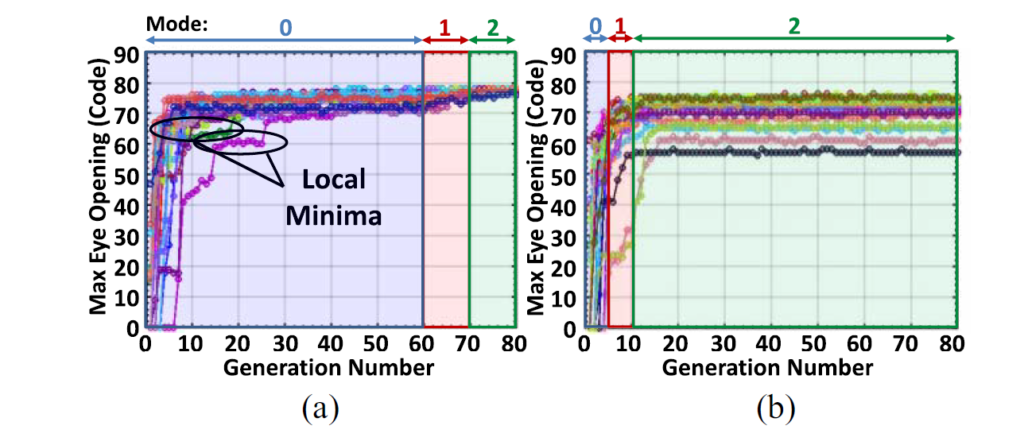
To visualize the efficiency of the genetic adaptation algorithm over the traditional gradient descent algorithms in avoiding local minima in the performance surface, Figure 7 shows the adaptation curves for 20 independent runs of the genetic adaptation algorithm (mode 0 and mode 1) followed by a gradient descent algorithm (mode 2) to track temperature and voltage variations. The maximum eye opening at each generation is plotted. In Figure 7(a), for some of the runs during mode 0 and mode 1, the coefficients converged to a local minimum, but over time they break out and converge toward the global minima. Figure 7(b) shows the adaptation curves for 20 runs when mode 0 and mode 1 are limited to only ten generations. It can be seen that when using gradient descent (mode 2), the coefficients fall in many different local minima due to different initial conditions and do not converge to the global minima.
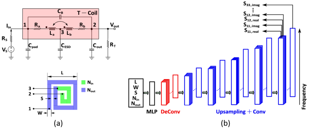
Taking a further step forward, we use machine learning (ML) in our design optimization research to further accelerate design iterations and predict the parameters of optimum designs. For example, we use a machine learning (ML) model to replace EM T-coil simulations, rapidly predicting the broadband S-parameters of a T-coil [5]. The T-coils are widely used in high-speed electrostatic discharge (ESD) circuits to increase bandwidth. However, T-coil modelling relies on time-consuming electromagnetic (EM) simulations, which precludes quick design space exploration and fast global optimization. Our proposed ML model is incorporated into a genetic algorithm (GA), affording a 10× speed improvement in optimizing a T-coil-enhanced ESD circuit compared to using traditional EM simulators, with reasonable accuracy of the proposed ML model. Figure 8(a) shows the model of a T-coil in an ESD circuit (upper side), and the layout of a T-coil (lower side). Figure 8(b) shows the proposed ML model architecture. The first multi-layer perception (MLP) section maps the input T-coil geometric parameters to some higher-dimension abstract representations. It is followed by an artifact-free deconvolutional layer and a series of upsampling convolutional layers. The final outputs are the real and imaginary parts of S11, S12, S13, S22, S23, and S33 from 100 MHz to 100 GHz with a frequency step size of 100 MHz.
Similarly, we are currently working on research that optimizes the interface interconnecting the photodetector and the analog front-end in high-speed optical receivers using a hybrid of analytical models, electromagnetic simulations, and a neural network-based model, in addition to a genetic algorithm to obtain optimal design parameters. The proposed optimization approach leads to a quick design time and reveals insight into best design practices. We used the proposed method to conclude the relationship between optimal transmission line width and analog front-end transimpedance on the one hand and the amount of equalization available on the other.
[1] L. Wang, Y. Fu, M. LaCroix, E. Chong, A. Chan Carusone, “A 64-Gb/s 4-PAM Transceiver Utilizing an Adaptive Threshold ADC in 16-nm FinFET,” IEEE Journal of Solid-State Circuits, Dec 2018. [On IEEExplore]
[2] M. Yang, S. Shahramian, H. Wong, P. Krotnev, A. Chan Carusone, “Global Optimization of Wireline Transceivers for Minimum Post-FEC vs. Pre-FEC BER,” DesignCon, August 2021. [PDF paper]
[3] Q. Yu, A. Chan Carusone, and A. Liscidini “Optimization of Quantized Analog Signal Processing Using Genetic Algorithms and u-Law,” IEEE Open Journal of Circuits and Systems, Feb. 2022. [On IEEExplore]
[4] B. Dehlaghi, S.Shahramian, J. Liang, R. Bespalko, D. Dunwell, J. Bailey, B. Wang, A. Sharif-Bakhtiar, M. O’Farrell, K. Tang, A. Chan Carusone, D. Cassan, D. Tonietto, “A 1.41pJ/b 56Gb/s PAM-4 Receiver Using Enhanced Transition Utilization CDR and Genetic Adaptation Algorithms in 7nm CMOS,” IEEE Solid-State Circuits Letters, 2019. [On IEEExplore]
[5] Z. Li, A. Chan Carusone, “Design and Optimization of T-Coil-Enhanced ESD Circuits with Upsampling Convolutional Neural Network,” International Microwave Symposium, Denver, Colorado, June 2022. [On IEEExplore]